TASKLED - Smart LED drivers
|
|
Operating Manuals (PDF) for H6Flex:
Drivers shipped after Jan 20, 2014:
Note: Sep 15, 2014. H6Flex V2.0 driver starts shipping. Schmitt Trigger filter circuit added to SWA input.
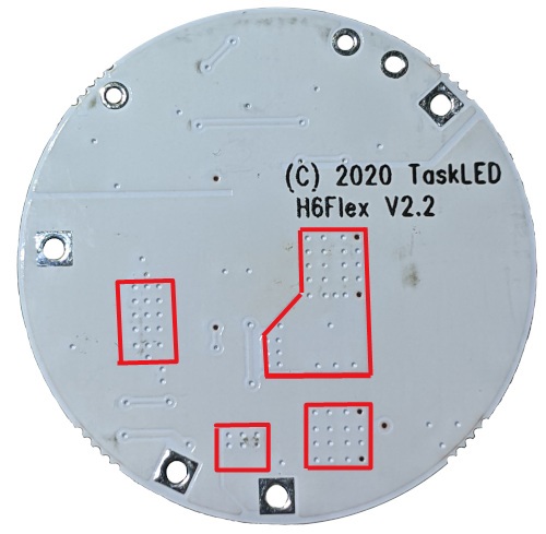
Technical Information:The picture below shows the bottom view of H6Flex. Marked areas on the bottom of the PCB are a direct thermal interface to the bottom of the power devices (on the component side of the PCB). If the power dissipation of the H6Flex board exceeds about 1W it is recommended to affix a heatsink or copper tab to a heatsink to the exposed areas using the supplied thermal pad material. The exposed areas are at various potentials and must NOT be electrically shorted or connected to the heatsink.
The supplied thermal pad material is nominally 0.25mm thick, white in colour and will conform to the heatsink and PCB surfaces to provide an excellent thermal path. Please ensure the heatsink and bottom of the H6Flex are cleaned of any grease or contaminants that would prevent the adhesive from properly bonding. Pressure should also be applied to help set the adhesive, refer to the datasheet for more information.
The thermal pad material (Li98 100 0.25mm) specifications can be found in the datasheet a copy of which is available here. The Li98 material provides a good compromise between the cost of the material and its thermal performance. The material is white in colour and has a protective cover on both sides that must be removed to expose the adhesive. Note, it is recommended to remove the Red protective material first and fix the pad to the heatsink or the H6Flex prior to removing the white protective material. The adhesive is an acrylic base and takes up to 24 hours for fully cure/set. After a few thermal cycles and 24 - 48 hours the bond will become stronger and the thermal conductivity will improve.
H6Flex V2.2
H6Flex V3.0 Updated microcontroller and QFN LED driver chip. No functional changes compared to V2.2 and V2.0

H6Flex V2.2
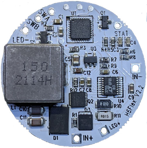
The circuitry (all surface mount) fits neatly on a 1.30" diameter PCB on the top side. The maximum board+component thickness of the driver is 0.35" where the inductor (L1) is situated. Note, the thermal pad material is nominally 0.039" thick, so total thickness would be 0.35" + 0.039" = 0.389".
The IN+ and IN- pads/holes are the input power connections to H6Flex. Pad hole diameter is nominally 0.055". 21V MAXIMUM input voltage (5 li-ion cells).
Input operating voltage range is 7V to 21V. H6Flex is capable (but not guaranteed) of running as low as 5V IF the LED current is configured to <= 1.4A.
The LED+ and LED- pads/holes are the output power connections from H6Flex to the LED load. LED- is NOT electrically the same as IN-. Pad hole diameter is nominally 0.055".
The STAT pin can be wired the the cathode of a status LED. Pad hole diameter is nominally 0.040". The anode of the LED should be wired to a current limiting resistor and then to IN+. It is the user's responsibility to calculate the necessary resistor value to limit the current to the LED. The resistor value can be calculated using the following equation.
Resistor_value = (VIN - STAT_LED_Vf) / STAT_LED_CURRENT
As an example, for 10mA to a Red LED with Vf of 2.5V and running from 16V battery voltage:
Resistor_value = (16 - 2.5) / 0.010 = 1350 ohms.
The SWA hole is one side of an external momentary action switch. The other side of the switch must be wired to SWB (which is electrically the same as IN-). The switch only switches a control signal and carries at most 350microamps. If using a magnetic reed switch, wire it across SWA and SWB. Pad hole diameter is nominally 0.040".
Note: it is recommended to keep the maximum wire length between the switch and H6Flex less than around 8 " (20cm). Having wire leads that are too long can cause the wires to act as an antenna and cause H6Flex to respond irregularly or turn on/off by itself.
Note, H6Flex is a Buck regulator (step down), so input voltage must be greater than the output voltage to ensure H6Flex remains in regulation. If the input voltage drops within 1V of the LED Vf (at the specified current) H6Flex will no longer regulate and the output voltage will drop and output current will also drop.The following table shows production board test results for UIP. The 7 current tables are listed across the top and each level (L1 to L5) for each current table is listed below (actual measured values). L1 to L4 are subject to change as necessary to optimise values, any changes would be minor tweaks to better 'linearise' the visual steps.
Level 1400mA 2000mA 2800mA 3600mA 5000mA 5600mA 6600mA L1 50mA 50mA 50mA 50mA 50mA 50mA 50mA L2 116mA 116mA 220mA 220mA 250mA 307mA 505mA L3 311mA 450mA 730mA 937mA 1105mA 1420mA 1620mA L4 680mA 1020mA 1593mA 2022mA 2450mA 3000mA 3377mA L5 1420mA 2022mA 2800mA 3610mA 5040mA 5640mA 6570mA
Some Efficiency Measurements:
The H6Flex driver has the H6CC switcher core (identical design), so the H6Flex efficiency will be the same as shown in the H6CC technical section.
Adequate heatsinking is essential when running at high output power.
To determine the heat being dissipated on the H6Flex driver, calculate the output power. Use the chart above to approximate the efficiency that the driver will be running at.
Lets assume 3 LEDs running at a nominal 2.8A from a 14.4V li-ion battery pack. From above we have the following:
Output_power = 3 x 3.5V x 2.8A= 29.4 Watts.
Efficiency is 93%, so losses in H6Flex are 7%.
Power dissipated as heat in H6Flex is 29.4 x 0.07 = 2.1Watts
This will require heatsinking via the thermal interface pad on the bottom of H6Flex.
As power being dissipated increases beyond 1W the thermal path to the heatsink becomes critical to reliable operation. Most of the heat being dissipated in the driver is from the power FET Q1, D1 and the inductor, L1. The thermal interface (bottom of the PCB) is tied directly to the bottom of Q1, D1 and L1 using thermal vias. Mounting an adequate heatsink with the supplied thermal pad material is recommended and will allow H6Flex to be run at high power reliably.
Tests performed with 5 Seoul P7 LEDs driven at 2.8A via H6Flex show that the H6Flex PCB temperature will be at most 15C hotter than the heatsink when used with the provided thermal pad material. These results were with H6Flex just resting against the thermal pad material (no pressure applied), so good performance without extra clamping force.
Magnetic Field Warning:
The H6Flex is a switching regulator based driver and contains a shielded Inductor (L1 in the picture above). Strong external magnetic fields such as from a magnet used to operate a Hall sensor or Reed switch can interfere with the Inductor's operation. It is recommended to maintain a minimum of 1" from the Inductor and any external magnet. If the magnet is very powerful, then the distance needs to be increased (more than 1") as needed to minimise interference to the Inductor.
Potting Warning:
Areas of the circuitry on H6Flex utilise high impedance paths and if potting (not required) is to be utilised, the user must ensure than the compound is non-conductive and non-capacitive (e.g. Arctic Alumina - NOT Arctic Silver) otherwise correct operation may be compromised. The same consideration is present if using thermal epoxy is used to mount the H6Flex driver to a heatsink.
Rather than potting, it is recommended to use the thermal interface pad on H6Flex to connect to a heatsink using the supplied thermal pad material. NOTE, the thermal interface area on H6Flex is NOT at ground potential.
Soldering to the thermal interface pad is NOT recommended.
home | products | technical | order products | contact
©2026 TaskLED. All Rights Reserved.